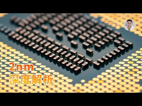

The 2nm Era: A New Chapter in Semiconductor Technology
The arrival of 2nm technology marks a significant leap in semiconductor manufacturing, not just in size reduction but also in the underlying technology used. This node represents a shift in approach, impacting major players like TSMC, Intel, Samsung, and Japan's Rebitus.
The Transition to GAAFET
The most crucial aspect of the 2nm node is the industry-wide adoption of GAAFET (Gate-All-Around Field-Effect Transistor) technology. This signifies the end of the FinFET era's dominance, as FinFETs are reaching their physical limitations. While FinFET will still exist, it is less than 3 nanometers.
-
FinFET Limitations: As transistor sizes shrink, the short-channel effect becomes more prominent, making it difficult to control current flow.
-
GAAFET Solution: GAAFET addresses this by completely surrounding the channel with a gate, providing superior control and mitigating leakage. This enables further miniaturization while maintaining performance.
From FinFET to GAAFET: A Historical Perspective
The evolution of transistor technology is driven by the need for better control over current as devices shrink.
- Planar Transistors: Early transistors had a flat structure with limited gate control.
- FinFET (around 2011): Professor Hu Zhiming of UC Berkeley proposed FinFET, offering three-sided gate control for improved switching performance. This became the standard for several generations.
- GAAFET: GAAFET takes this further by creating a gate that surrounds the channel on all four sides, offering even better control. This is achieved by stacking nanosheets within the transistor.
TSMC's N2 Process and Logic Density
At the 2nm node, TSMC's N2 process stands out, with a logic density exceeding 300 million transistors per square millimeter. Logic density and SRAM density are key metrics, but they have different scaling characteristics.
-
Logic Density: Refers to the density of logic circuits.
-
SRAM Density: Refers to the density of static random-access memory. SRAM is more difficult to shrink due to its architecture.
TSMC claims its 1.15x density improvement is compared to N3E (the second generation 3nm). Logic density across different nodes:
-
5nm: Approximately 170
-
3nm (N3B): Approximately 290
-
3nm (N3E): Approximately 270
-
2nm (N2): Currently 313
The enhancement may not be as substantial as the shift from 5nm to 3nm, it's still a milestone.
Comparing TSMC, Samsung, and Intel
While all three companies are pursuing 2nm technology, TSMC's N2 currently offers a higher logic density than Samsung's SF2 (238) and Intel's A18 (estimated 238). Future iterations like N2P, A16, and A14 from TSMC are expected to push the boundaries further, potentially exceeding 400.
Challenges and Innovations
The transition to GAAFET requires redeveloping process experience accumulated during the FinFET era. The complex structure of GAAFET necessitates precise multi-layer quantization growth and testing.
-
Stability over Aggression: The initial focus is on stability rather than aggressive density targets.
-
SRAM Density Improvement: GAAFET allows for lower operating voltages, which enables further improvements in SRAM density.
Future Technologies: Back-End Power and Hi-NA EUV
Further improvements in density and performance will require new technologies.
-
Back-End Power Delivery: Relocating power cables to the back of the chip to free up space for signal lines and optimize standard cell layout.
-
Hi-NA EUV: Introducing extreme ultraviolet lithography with higher numerical aperture (Hi-NA EUV) for increased resolution and smaller feature sizes.
NanoFlex Technology
TSMC is utilizing NanoFlex technology in the N2 process, building upon the FunFlex introduced in N3. NanoFlex adjusts the width of the nanosheets in GAAFETs, enabling optimization for low power consumption (narrow chips) or high performance (wide chips). This allows for customized circuit designs within a single chip.
Conclusion
The 2nm node represents a pivotal moment in semiconductor technology, marked by the shift to GAAFET and the ongoing pursuit of higher density and performance. While challenges remain, the innovations being implemented pave the way for further advancements in the years to come. Despite all companies going down the GAAFET path, TSMC's N2 process is the only one that is considered to truly represent the 2nm node.
 {#
{#  {#
{#  {#
{#  {#
{#  {#
{#