
Understanding High Bandwidth Memory (HBM)
This article explores High Bandwidth Memory (HBM), a crucial technology driving advancements in Artificial Intelligence (AI). We'll delve into what HBM is, how it works, its advantages, and the current state of the HBM market.
What is HBM?
HBM stands for High Bandwidth Memory. It's a type of DRAM (Dynamic Random Access Memory) used in applications requiring high performance, like GPUs (Graphics Processing Units) for AI and machine learning. While similar to LPDDR, DDR, and GDDR memory found in phones, computers, and graphics cards, HBM boasts a unique architecture that provides significantly higher data transfer rates.
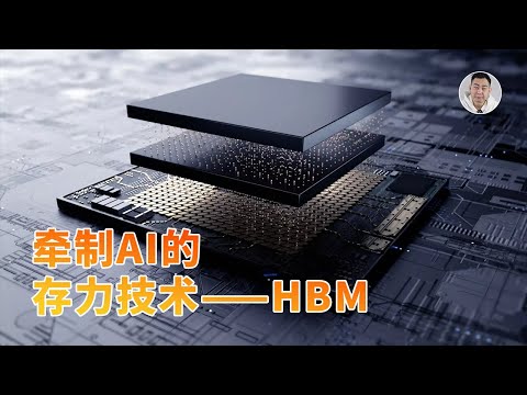
HBM's Unique Architecture
Unlike traditional DRAM, which uses a flat layout, HBM employs a three-dimensional stacked structure. This consists of multiple layers of DRAM dies, typically 4, 8, or 12, stacked directly on top of each other.
-
DRAM Die: These layers are responsible for data storage.
-
Logic Die: Located at the bottom, this chip controls the storage units, handling signal processing, read/write operations, and power management.
-
Interposer Layer: Connects the HBM stack to the CPU, GPU, or System on a Chip (SoC).
-
Silicon Base: Provides the foundation for the entire structure.
This stacked configuration enables HBM to achieve significantly higher bandwidth compared to traditional DRAM.
Key Technologies Behind HBM
The manufacturing of HBM involves two crucial technologies:
-
TSV (Through-Silicon Via): This is a back hole technology used to create vertical connections through the DRAM layers for signal and power transmission. Creating these "holes" is extremely challenging, requiring precision and uniformity at the micrometer scale.
-
MU-BUMP (Micro-Bump): This is a connection technology used to bond the stacked DRAM layers and connect them to other components.
The Advantage of High Bandwidth
HBM's high bandwidth stems from its wide data path, typically 1024 bits. This is achieved by dividing the memory into multiple logic channels, each with a certain width (e.g., 128 bits). The total bandwidth is the sum of the bandwidth of each channel (e.g., 8 channels x 128 bits = 1024 bits).
In contrast, GDDR memory, even the most advanced GDDR7, has a significantly smaller data path (e.g., 32 bits). While GDDR focuses on high frequency and low bandwidth, HBM prioritizes low frequency and high bandwidth. This architecture makes HBM particularly well-suited for AI applications that demand rapid data access.
HBM vs. GDDR: A Comparison
| Feature | HBM | GDDR |
|---|---|---|
| Architecture | 3D Stacked | Flat |
| Bandwidth | High | Lower |
| Frequency | Low | High |
| Data Path Width | Wide (e.g., 1024 bits) | Narrow (e.g., 32 bits) |
| Power Consumption | Low | Higher |
| Applications | AI, high-performance computing | Gaming, graphics cards |
HBM offers significant advantages due to its low power consumption, short signal delay, and compact size.
Addressing the "Memory Wall"
HBM plays a vital role in alleviating the "memory wall" problem, where the speed of data transfer between memory and the processor becomes a bottleneck. Because modern computers have a data separation design, data must frequently move between computing and storage devices. HBM's high bandwidth allows GPUs to access data more quickly, enabling them to perform complex calculations for AI applications more efficiently.
The Rise of HBM in the AI Era
The emergence of AI has fueled the demand for HBM. Its architecture and high bandwidth capabilities are ideally suited for the data-intensive tasks involved in AI training and inference.
The HBM Market Landscape
The HBM market is dominated by three key players:
-
SK Hynix: Considered a leader in HBM technology.
-
Samsung: A strong competitor in the HBM market.
-
Micron: A relative newcomer but quickly catching up.
SK Hynix established an early lead by partnering with AMD and later becoming a major supplier to Intel. Micron initially invested in an alternative technology called HMC (Hybrid Memory Cube) but later shifted its focus to HBM.
The Future of HBM
The HBM market is expected to grow significantly in the coming years. HBM4, the next generation of HBM, is already under development, promising even higher performance and efficiency. Companies like SK Hynix and TSMC are exploring innovative integration techniques to further improve HBM performance.
China's Progress in HBM
China is actively working on developing its own HBM technology. While HBM2 is already said to be mastered, HBM2E is expected to be complete by 2026.
 {#
{#  {#
{#  {#
{#  {#
{#  {#
{#